GP
Great PlasticsEngineering Materials & Custom Parts
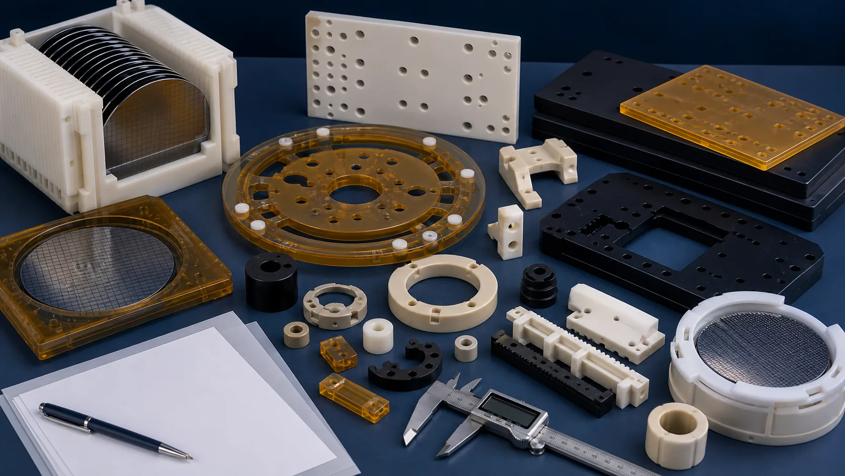
Semiconductor Engineering Plastics
Semiconductor engineering plastics for wafer handling, wet process and precision tool parts.
Compare PEEK, PTFE, PFA, PVDF, PEI, PI, PPS and ESD plastics for clean process fixtures, wafer-related carriers, wet chemistry parts, insulators, spacers, vacuum-tool components and machined precision parts.
Short answer
Semiconductor plastic selection starts with process zone risk.
Semiconductor engineering plastics are chosen by process environment, not material name alone. A wet bench guide, wafer handling fixture, ESD support, vacuum-tool spacer or thermal-zone insulator may need different priorities: chemical resistance, low particle generation, low outgassing, dimensional stability, electrical behavior, machinability, surface finish and documentation. The page below turns those requirements into practical material and RFQ decisions.
Application matrix
Common semiconductor engineering plastics project types.
| Project context | Typical parts | Material directions | Review before quote |
|---|---|---|---|
| Wet process and chemical exposure | Guides, spacers, carriers, manifolds, plates, fluid path supports | PTFE, PFA, PVDF, PEEK, PPS, PP | Chemicals, concentration, UPW, temperature, cleaning cycle and surface condition |
| Wafer handling and positioning | Carriers, nests, edge-contact parts, locating pads, guide rails | PEEK, PEI, POM, PPS, ESD grades | Particle risk, contact surface, tolerance, wear, ESD target and burr control |
| Electrical insulation and ESD control | Insulators, standoffs, plates, housings, tool supports | PEI, PEEK, PI, PPS, ESD PEEK, ESD acetal | Insulation or dissipative target, heat, voltage context and dimensional stability |
| Vacuum and thermal tool zones | Spacers, rings, covers, supports, test fixtures | PI, PEEK, PEI, PPS and selected high-performance grades | Temperature, vacuum, outgassing concern, load, thickness and inspection points |
| Prototype and replacement work | Machined samples, replacement parts, fixture updates, low-volume components | Material matched to drawing, tool zone and failure mode | Revision level, sample wear, surface finish, packaging, quantity and lead time |
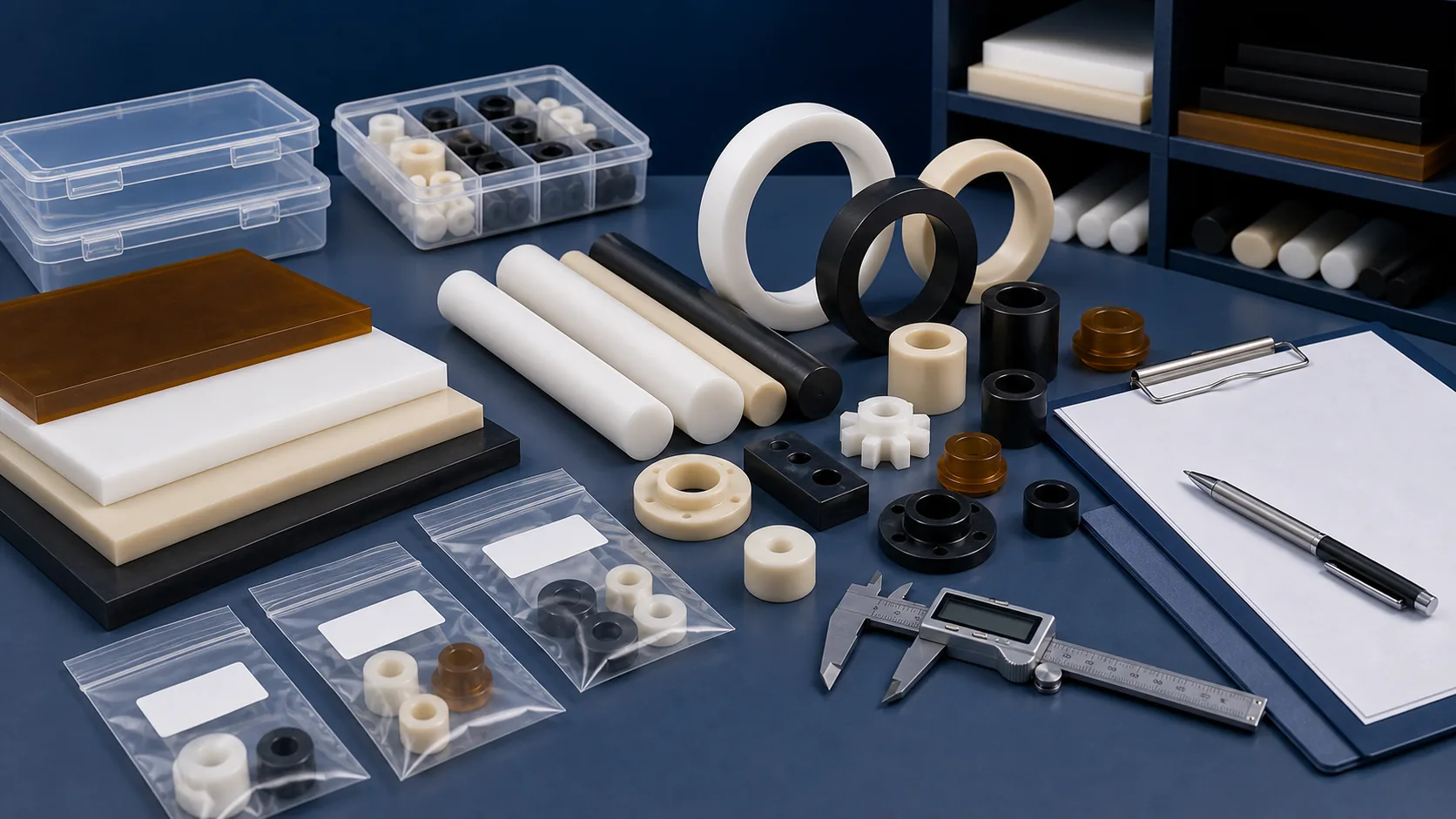
Material choices
Materials commonly reviewed for semiconductor plastic components.
PEEK
Reviewed for structural process parts, precision fixtures, wear features and higher-temperature components where strength and stability matter.
PTFE and PFA
Used where chemical inertness and wetted-zone performance are the primary drivers, while creep, tolerance and mechanical load need review.
PVDF
Often considered for wet process fixtures and fluid handling parts that need chemical resistance with more stiffness than many fluoropolymers.
PEI
Useful for rigid, heat-resistant insulators, fixtures and transparent amber parts where dimensional control is important.
PI and PPS
Reviewed for higher-temperature, insulation, dimensional stability or chemical environments when the process zone demands more than standard plastics.
ESD materials
Considered when static control matters, with surface resistivity, cleanliness, machining behavior and part contact risk checked together.
Selection path
Translate process requirements into a material shortlist.
| Decision point | What to define | How it affects material and process |
|---|---|---|
| Wet chemistry | Chemical list, concentration, UPW exposure, cleaning agents, temperature and dwell time | Separates PTFE/PFA/PVDF/PEEK/PPS/PP options and flags swelling, creep or machining concerns |
| Particle and surface risk | Wafer contact, sliding surface, burr sensitivity, finish and cleaning expectations | Influences material grade, machining strategy, edge design, deburring and packaging notes |
| Electrical behavior | Insulating, conductive or static dissipative need, voltage context and contact sensitivity | Determines whether ESD grades, PEI, PEEK, PI, PPS or another family should be reviewed |
| Thermal or vacuum zone | Temperature, vacuum, purge gas, exposure time, load and thickness | Pushes the review toward PI, PEEK, PEI or PPS and changes inspection or data needs |
| Geometry and tolerance | Thin walls, slots, wafer edge contact, bores, flatness, threads and critical surfaces | Determines whether CNC machining from sheet, rod, plate or tube is the practical route |
Failure review
Small drawing omissions can create process-tool problems later.
Semiconductor plastic parts often look simple on a drawing, but process zones add risk. A slot edge can generate particles, a tight bore can move after thermal exposure, a wet process plate can creep under clamping load, or an ESD part can be specified without the electrical target. Early RFQ details help separate material, geometry and process risks before machining begins.
- Particle generation from burrs, sharp edges, sliding contact or unsuitable surface finish.
- Dimensional movement from heat, moisture, chemical exposure, stress relief or thin sections.
- Wrong electrical behavior because insulation, conductive and dissipative needs were not separated.
- Outgassing or contamination concerns added after material, cleaning or packaging was already quoted.
Manufacturing route
Choose the route around precision, surface and project stage.
CNC machining
Useful for fixture plates, carriers, spacers, insulators, vacuum-tool parts, prototypes and low-volume precision components.
Cut blanks and stock shapes
Sheets, rods and tubes support early material review, carrier plates, spacers, rings, covers and emergency replacement work.
Repeat production planning
When part geometry stabilizes, review fixture strategy, edge finishing, inspection points, packaging and revision control.
RFQ checklist
Details that make a semiconductor engineering plastics quote more useful.
| RFQ input | What to send | Why it matters |
|---|---|---|
| Drawing package | 2D drawing, 3D model, revision level, critical surfaces and sample photos | Defines tolerance, wafer-contact geometry, edge finish, flatness and machining route |
| Process zone | Wet chemistry, UPW, temperature, vacuum, ESD target, cleaning and packaging needs | Connects material choice to the actual tool environment |
| Performance target | Particle sensitivity, wear surface, stiffness, insulation, dissipative behavior and expected life | Prevents material choices based only on a generic high-performance plastic name |
| Commercial and quality needs | Quantity, project stage, lead time, inspection points, documents and packaging notes | Aligns prototype, replacement and repeat production planning before quoting |
FAQ
Questions buyers ask about semiconductor engineering plastics.
Which plastics are commonly used for semiconductor engineering plastics?
PEEK, PTFE, PFA, PVDF, PEI, PI, PPS and selected ESD grades are commonly reviewed depending on wet chemistry, temperature, vacuum, particles, outgassing, stiffness, wear and electrical behavior.
How do I choose plastic for wafer handling or wet process parts?
Start with the process environment: chemical media, UPW exposure, temperature, wafer contact, particle risk, ESD or insulation need, outgassing concern, tolerance, surface finish and documentation requirements.
Can semiconductor plastic components be CNC machined?
Yes. CNC machining is useful for fixture plates, carrier parts, spacers, guides, insulators, vacuum-tool components, prototype parts and low-volume precision parts when drawings or 3D models are available.
What RFQ details matter for low outgassing plastics?
Include the operating temperature, vacuum or purge environment, exposure duration, material target, geometry, surface finish, cleaning or packaging needs, quantity and any requested data or inspection points.
Why do semiconductor plastic parts fail in process tools?
Common issues include wrong chemical compatibility assumptions, particle generation from wear or burrs, dimensional movement, electrostatic concerns, outgassing in thermal or vacuum zones, sharp corners, and missing surface finish or cleaning notes.
Related pages
Continue the semiconductor plastics review.
Semiconductor plastics RFQ
Send the drawing with process-zone, surface and documentation details.
Include material target, part function, drawing or 3D model, wet chemistry, UPW, temperature, vacuum or ESD needs, critical surfaces, tolerance, finish, quantity, packaging and lead-time target.